Menu
Close
Sign up for NPL updates
Close
Sign up for NPL updates

For people, place, prosperity and planet, we deliver impact with measurement science

Quantum technologies

Nanoscale magnetics consultancy

Characterisation of magnetic properties

This service is aimed at companies developing new spintronic devices and manufacturers assessing the magnetic properties of materials in production.  It will also be of interest to researchers and universities studying fundamental magnetic properties. NPL offers a range of services aiming to help solve some of the following problems:

  • Manufacturing defects
  • Unreliable magnetisation switching 
  • Magnetic properties not  meeting specifications
  • Test and evaluation for magnetic sensor development 
  • Poor magnetic sensor performance
  • Sub-optimal cross-talk between devices on the same integrated circuit
  • Assessing the quality of supplier magnetic nanoparticle materials 
  • Grain scale effects adversely impacting performance different steel batches conveying dissimilar properties

Imaging magnetic properties on the nanoscale

NPL has several specialised techniques allowing characterisation of devices and materials’ magnetic properties on the nanoscale. We offer consultancy services using a range of state-of-the-art techniques.

Read the recent article about NPL’s work in this area: Magnetic Force Microscopy: Comparison and Validation of Different Magnetic Force Microscopy Calibration Schemes

Find out more about NPL's Magnetics product and services

Find out more about NPL's Advanced materials product and services

Find out more about NPL's Low-loss electronics research

Contact us

Magnetic force microscopy

Standard magnetic force microscopy (MFM) provides qualitative mapping of a sample’s magnetic stray field at the surface. Nanoscale characterisation of magnetic fields is important for fundamental and applied research on magnetic materials and devices. It includes:

/getattachment/cf23d604-eb5e-4642-981f-c74baac7b9c4/Magnetic_portable_microscopy.png?lang=en-GB

  • Understanding of domain structure in magnetic materials
  • Understanding of the origin of magnetic losses in electrical steels for electric motors or transformers
  • Characterisation of local fields for magnetic sensors and devices for consumer electronics.

​NPL has developed a new method to offer quantitative MFM measurements which provides quantitative values of the stray field. This unique MFM scanning technique can be combined with other systems and techniques to allow:

  • In-field measurements, with up to 150 mT of in-plane or 100 mT of out-of-plane field
  • Electrostatic compensation using Kelvin-probe microscopy (KPFM), ideal for electrically biased devices or other materials where the surface charge is important,  especially for 2D semiconductor materials
  • Measurements in a range of environmental conditions, such as vacuum down to the 10-6 mbar or up to 100 °C
  • Capability to electrically monitor the sample while imaging, which allows the study of local electrical, magnetic or thermal gating effects
Nitrogen vacancy magnetometry

Nitrogen-vacancy (NV) based sensing represents a breakthrough paradigm in characterising advanced quantum material systems. Combining the NV-sensor into a scanning probe microscope (SPM) creates the ability for spatially resolved quantum sensing of physical phenomena and represents an extremely powerful and versatile measurement tool.  

Magneto-optical Kerr effect

/getattachment/1648afae-81f6-4c17-bdad-b6c934bf6a9f/Magnetooptical_kerr_effect.jpg?lang=en-GBThe magneto-optical Kerr effect (MOKE) system at NPL has a field of view of a few mm down to a resolution of 200 nm, and allows the study of the surface magnetisation of a wide range of samples, with both in-plane and out-of-plane fields. We can examine thin films, magnetic devices, and bulk materials to:

  • Understand domain structure in magnetic materials
  • Investigate the origin of magnetic losses in electrical steels for electric motors or transformers
  • Study quantum spintronic materials and devices, e.g. relevant for magnetic memories, magnetic sensors, radio-frequency and microwave devices, logic and non-Boolean devices.
Magneto-transport measurement system 

/getattachment/9ed0ba79-4f95-4bfb-8c14-c78b0e64cc67/Magnetotransport.png?lang=en-GBOur magneto-transport measurement system allows measurement of in-field electrical properties of magnetic devices, magnetic sensors and materials whose electrical properties are susceptible to magnetic fields. The system operates at room temperature and allows 360° rotation of the sample in the field. Measurements can be performed in fields up to 2 Tesla with both DC and AC Currents or voltages up to 50 MHz. This system allows: 

  • development of magnetic field sensors 

  • investigation of magnetisation evolution in nanodevices 

  • measurement of carrier properties in 2D materials.  

The system can also be utilised with the Keithley 4200 Semiconductor analyser for evaluation of highly resistive devices with fast turnaround. 

Physical Property Measurement System

Characterisation of quantum materials and devices

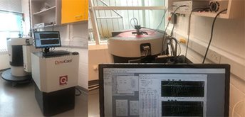
A comprehensive Physical Property Measurement System (PPMS) underpinning the characterisation of advanced electronic and magnetic materials and devices. With a broad temperature range and an ability to apply high magnetic fields, the system is particularly suitable for characterisation of quantum materials and devices.  With fast cool down times and stable magnetic field ramping, measurement time can be fully utilised reducing the cost to customers. From industry and SME’s to academia, the PPMS is a versatile tool for detailed characterisation of bulk samples, micro and nanofabricated devices, as well as nanoparticles, for developing future quantum and nanoelectronics technologies.  

The DynaCool PPMS’s flexible design combines many features in one instrument, including magnetometry and electrical transport measurements as well as ferromagnetic resonance spectroscopy. The system can work in a wide range of magnetic fields (up to 9 Tesla) and temperatures down to 1.8K with no need for liquid cryogens (cryogen-free) resulting in significantly reduced running costs compared with traditional wet cryogenic systems.

Magnetometry  

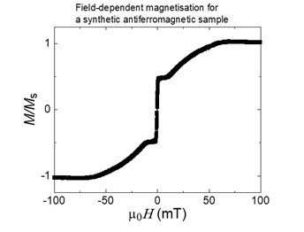
Vibrating Sample Magnetometer (VSM)  
The VSM option enables measurement of a sample's magnetic moment as a function of temperature or magnetic field.

AC Susceptibility
The AC measurement system utilizes a mutual induction-based technique to determine a sample's dynamic (AC) susceptibility.

Electrical Transport

AC Resistance
The electrical transport option enables AC electrical transport measurements of samples using a 4-probe lead configuration, suitable for all ranges of samples, but especially useful for looking at resistive samples, or those where pulsed current measurements could be utilised such as when studying memristors.

DC Resistance
The PPMS can measure DC resistance on up to three channels using a standard puck. This option highlights the efficiency of this system, with data for full temperature and field sweeps of three samples taken simultaneously, reducing the time cost even further.

Ferromagnetic resonance (FMR)

Broadband FMR spectroscopy utilising the NanOsc CryoFMR-40 allows for dynamic property measurements up to 40 GHz. FMR over such a wide frequency range enables the extraction a variety of magnetic parameters, several which are traditionally inaccessible by static measurement techniques, as well as extracting parameters which can be correlated with those derived from static measurements. From FMR we can extract;

  • Calculates the effective magnetization (Meff), anisotropy (K), gyromagnetic ratio (γ), damping (α), and inhomogeneous broadening (ΔHO)
  • Enables the user to extract the exchange stiffness (A) and inverse spin Hall effect ISHE (e.g. spin Hall Angle (θSHA)).

All of these are crucial in developing materials for integration into next-generation Low Loss Electronics.

Contact our quantum team


Physical Property Measurement System 

Confidence in product development

NPL experts can provide consultancy in the field of spintronics and quantum materials.
As well as the techniques above, we can help with:/getattachment/b81181b3-e61f-4d78-abf8-787aac13e627/Confidence.png?lang=en-GB

  • Nanoscale thermal and electrical measurements
  • Nanofabrication design
  • Electron-based detection, such as electron holography and Lorentz microscopy
  • Numerical simulations
  • Communicating with standards organisations
200mm environmental probe station

200mm environmental probe stationFor up to wafer scale measurements, we use a Suss PM8 Probe station equipped with 4 DC coaxial probes. The system benefits from a light tight, EM shielded enclosure with gas purging capabilities and a hot chuck up to 200 °C, for environmental testing.  

The system can be used for electrical measurement in the DC regime and with AC currents/voltages up to 50MHz.  

The system is also equipped with 2 microwave standard Ground-Signal-Ground probers for high and RF frequency measurements up to 40 GHz. A new, additional capability, expected June 2024, will be pulsed electrical measurements with ultra-fast rise time <200 ps and short pulse widths up to 100 ns, the type of measurements typically used in future memory devices or alternative low-power computing. 

Adaptations are being made to both the Magnetotransport Measurement System and the Probing capabilities to seamlessly integrate the two systems for measurements in magnetic field. 

Measurement for Quantum

Removing barriers to innovation

Announcing a new programme to support the UK quantum industry through access to specialist science and engineering advice and facilities.

Learn more

Contact us

Our research and measurement solutions support innovation and product development. We work with companies to deliver business advantage and commercial success.
Contact our Customer Services team on +44 20 8943 7070