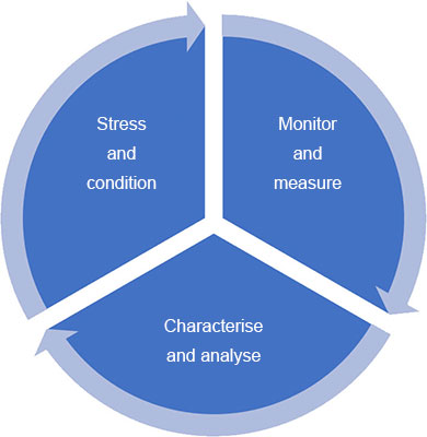
Many companies perform reliability prediction tests as an integral part of their development process, to ensure their products will survive in the field over the intended design lifetime. The challenge is to design tests which are as effective as possible in identifying and preventing the vulnerabilities that could result in failure.
Most companies have honed their testing to reflect the environments into which their products are deployed. We go further and address the challenges which come with:
We have extensive hands-on experience and are familiar with the most pertinent failure mechanisms and the most appropriate testing regimes.
Our experts are able to stress electronics and continously monitor the effect of varying temperature, current and environment. Rapid analysis of faults enables changes to be made and designs adapted to make the devices more reliable and robust.

Stress and conditionThermal shock (to 300°C) |
Monitor and measureConstant continuity monitoring (max 900 channels) |
Characterise and analyseFIB (Focused Ion Beam) |
Don’t see what you are looking for? Our diverse skill set enables us to provide bespoke solutions. Please contact us to discuss your requirements.
Our research and measurement solutions support innovation and product development. We work with companies to deliver business advantage and commercial success.
Contact our Customer Services team on +44 20 8943 7070