
 NPL has created a patented contactless, fast and in-line conductivity and sheet resistance measurement capability for advanced materials such as thin films, graphene and semiconductors. We can offer access to this through consultancy or also licensing of our intellectual property.
 Graphene’s unique electrical properties are key to many of the most promising future applications of this unique material. The production of high quality large areas of graphene and other 2D materials are critical for such applications, however each new set of growth parameters and transfer techniques requires characterisation to understand the effect the processes have on the quality of the graphene and other 2D materials.
Here at NPL we have invented (and patented) a method for characterising thin film electrical properties which is non-invasive and fast. Being non-invasive means you can measure the conductivity of the graphene/thin film sample without touching it (normal methods require either patterning the thin film or contacting it with probes and both of these have to be done off-line). Our technology is fast, a single measurement takes a fraction of a second so you can be monitoring the quality of the material as it flows off the production line, even at a rate of metres/minute, in principle.
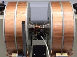
The microwave dielectric resonator system is self-contained and is potentially usable in relatively harsh environments. In addition, as well as conventional electrical sheet resistance measurements a version capable of electrical mobility and charge carrier concentration is under development.
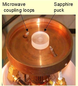
Graphene's high conductivity and low thickness enable a unique non-contact technique for measurement of sheet resistance, using a technique based on perturbation of a microwave dielectric resonator [1-4].
 The bare cavity resonance is at 10.6 GHz. It will require measuring a plain substrate and the target 2D film on a single side of an identical substrate, e.g., quartz, SiC, PET, glass, Si. We can complete the measurement under ambient conditions and this will take approximately 2-3 minutes. The closed cavity technique can measure a large sheet resistance range: 50 Ω/sq to 1 MΩ/sq.
Uniform mono- or a few layer 2D films on a single side of a low-loss substrate.
Sample size in between 3×3 mm2 and 12×12 mm2
Substrate thickness in between 200 µm to 1000 µm
The ratio of the film’s area to the substrate area should be ideally one (full coverage), otherwise it must be accounted for in calculating the sheet resistance
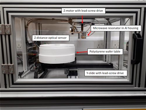
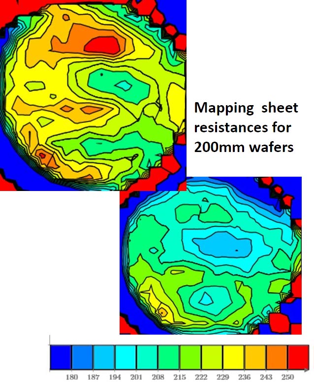
The NPL automated wafer scanning system [5-7], measures the target 2D film on a single side of a substrate, e.g., quartz, SiC, PET, glass, Si, in comparason with a plain substrate of the same material. The dielectric resonator frequncy is at 3.5 GHz. We can complete the measurement under ambient conditions. Scan time is 100 ms per step. A typical wafer-scale test duration is 20 min. Spatial variation in the sheet resistance (through linewidth) and dielectric environment (through frequency shift) can be mapped. Spatial resolution depends on the opening: 5 to 20 mm. Flexible measurement scheme: the film-covered side of the substrate can face up or down. The system is capable of measuring a large sheet resistance range: 50 Ω/sq to 1 MΩ/sq.
Sample restrictions:
Max wafer diameter is 250 mm
Substrate thickness may be up to 10mm
 The Microwave Resonator can offer a series of benefits to organisations invovled in producing or developing next generation advanced materials or products related to Graphene/2D materials, thin films (including. batteries, coatings (optical and protective), displays (ITO film) and electronics.
The issue of non-invasive electrical measurement is common to a wide range of manufacturers in digital electronics, communications and semiconductor fabrication sectors. The cost of rejected wafers or other mass produced batch samples can be significant. The ability to monitor in-line production with no need to remove samples for batch testing can bring enormous cost savings and improved quality of end product.
Measurement of the electrical properties of thin films is an increasingly demanding issue for fabrication of large scale electrical components, both active and passive. Quality control demands accurate measurement of e.g. sheet resistance over large wafer scale production. High speed, combined with non-invasive measurement, are critical.
The microwave resonator technique is applicable across a range of spatial resolutions, from millimetres to micrometres. An entire 200 mm diameter wafer can be scanned at 10mm resolution (500 measurements) in ~ 10 minutes for present prototype system.
Our research and measurement solutions support innovation and product development. We work with companies to deliver business advantage and commercial success.
Contact our Customer Services team on +44 20 8943 7070