Hall effect measurements to characterise electrical properties of advanced materials and devices
NPL has electrical measurements services capable of characterising the electrical transport properties: the electrical resistivity (or conductivity), majority carrier type (electrons or holes), charge carrier density and mobility. These measurements can be done in a wide range of conditions:
- ambient
- vacuum (down to 10-5 mbar pressure)
- controlled relative humidity (0 to 80%)
- over a wide temperature range (2 K to 400 K)
- controlled gas environment
- large magnetic field capability (±9 T)
- DC or AC (up to 100 kHz) electrical excitation.
NPL’s capabilities enable the development and optimisation of new devices to be accelerated, including for environmentally-sensitive applications.
The measurements can be done using two techniques:
-
Custom-built electrical transport measurements in variable environments setup (ETMiVE),
-
Quantum design physical properties measurement system (PPMS).
Both systems enable:
- Quick and reliable identification of the electronic properties of continuous films without the need for expensive and time-consuming patterning
- Monitoring of the electronic properties which are dependent on short- and long-term environmental changes
- The response of advanced materials to be monitored as changes are made in environmental pollutants
Electrical transport measurements in variable environments setup (ETMiVE)
The custom-built setup is capable of electrical transport measurements in the following conditions:
Ambient
- Vacuum (down to 10-5 mbar pressure)
- Controlled relative humidity (0 to 80%)
- Controlled gas environment
- Temperature ranging from 300 K to 400 K
- Magnetic field range of ±25 mT
- AC electrical excitation (up to 100 kHz)
The electrical transport measurements are automated and can be performed continuously in a fixed or varying environment. Further customisation is possible upon request, such as 2-wire device measurements, DC excitation and mixed gas environments.
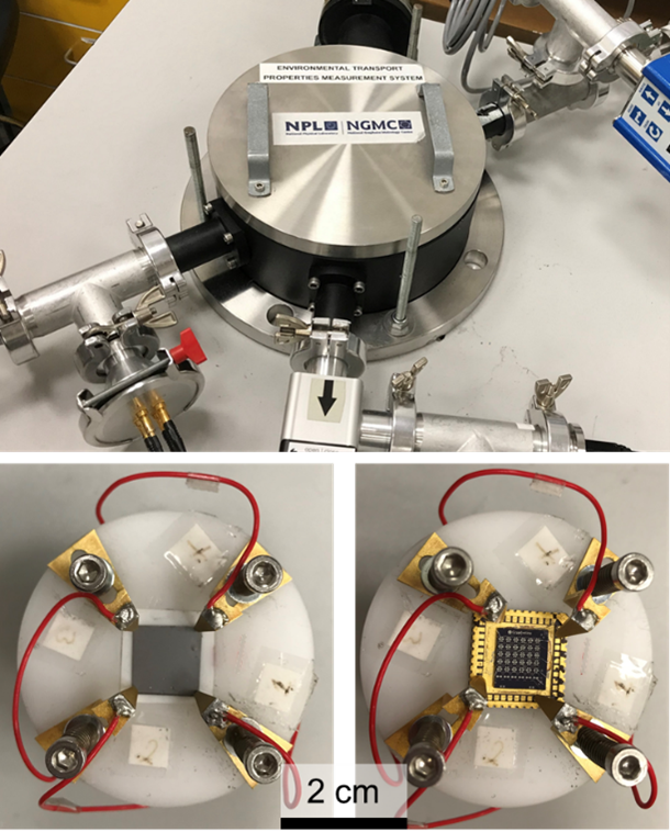
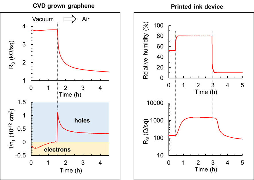
Measurement chamber (top). Sample holder probing a continuous conductive film (bottom – left) and a microscale device on a chip (bottom – right). The electrical contacts of the microscale device are extended to a chip carrier via wire bonding. | Representative results from a CVD grown graphene film on SiO2 (left) and a water-based conductive ink printed on a glass substrate (right). The environment changes from vacuum to air for the graphene sample (left). The response in the electrical properties is very clear: the sheet resistance drops and the majority carrier type switches from electrons to holes. For the printed ink device, the relative humidity is varied between 80% and 10% (right). Orders of magnitude change in the sheet resistance is captured as a result. |
.png?lang=en-GB "/getattachment/9071776f-82e3-431e-b201-14e371173e8e/etmive1-(1).png?lang=en-GB")
Physical Properties Measurement System (PPMS)
PPMS is able to perform the electrical transport measurements in the following conditions:
Temperature ranging from 2 K to 400 K
Magnetic field range of ±9 T
- Low pressure He environment (10 mbar at 300 K)
- DC and AC electrical excitation (up to 200 Hz)
- Simultaneous measurements of up to 3 devices
Custom electrical measurements are available by integrating external measurement equipment with PPMS, such as transistor measurements, 2-wire device measurements.
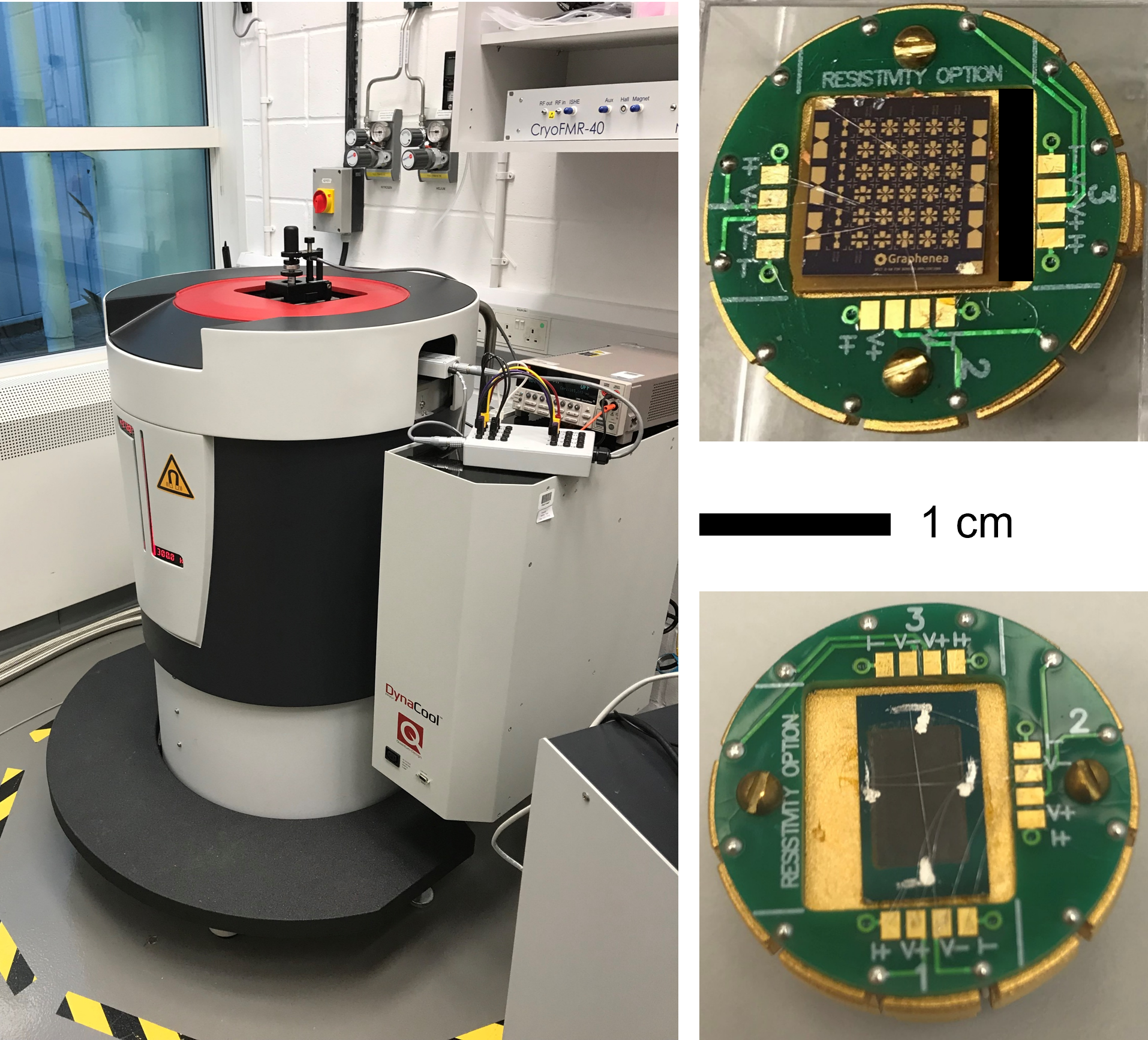
PPMS (left) and its sample holder with a graphene FETs chip (top – right) and a thin film on SiO2/Si substrate (bottom – right)
|
Representative PPMS results: Temperature-dependent mobility for 3 different materials: a graphene Hall bar device (top), a composite film (middle), conductive ink printed on a glass substrate (bottom). |
.png?lang=en-GB "/getattachment/d69ea414-bc43-428c-a37b-b1e9e04208d9/etmive2.png?lang=en-GB")

Exploring quantum photodetectors at cryogenic temperatures
Empowering nanoscale precision: First Graphene breakthrough in conductivity measurement
Electrical tests in cryogenic and variable environments
Validating the effectiveness of thermal paints at high temperatures and humidity
Revealing new markets for graphene sensors
New metrology unlocks potential sales for advanced materials innovator
An unparalleled range of measurements
Capability |
ETMiVE |
PPMS |
Temperature range |
300 K to 400 K | 2 K to 400 K |
Conditions |
|
|
Electrical excitation |
AC (up to 100 kHz) | DC, AC (up to 200 Hz) |
Magnetic field |
±25 mT | ±9 T |
Simultaneous measurements |
1 | 2 for AC, 3 for DC |
Sample dimensions |
< 1 cm | < 1 cm |
Sample type |
van der Pauw | van der Pauw Hall bar |
Upper R limit |
0.1 MΩ | 1 MΩ |
Lower mobility limit |
10 cm2 V-1 s-1 | < 1 cm2 V-1 s-1 |
For van der Pauw measurements:
- The sample must be homogenous, continuous, and isotropic
- The thickness must be uniform
- The film thickness must be known for calculation of the resistivity (conductivity) and volume carrier density.
Applications
The service could support the following applications and sectors:
- 2D materials, e.g., single and multi-layer graphene - Case Study: Validating the Effectiveness of Shielding and Thermal Paints at High Temperatures and Humidity
- Devices: Hall bar, Hall sensors, transistors, memory devices (e.g., RRAM) - Case Study: Revealing New Markets for Graphene Sensors
- Printed Electronics
- Conductive inks/pastes
- Thin film photovoltaics: Si, CdS/CdTe), CIGS, perovskites
- Organic films and electronics
- Transparent oxides
- Thin-film transistor materials (Si, IGZO)
- Sensing materials and sensors
Contact us
Our research and measurement solutions support innovation and product development. We work with companies to deliver business advantage and commercial success.
Contact our Customer Services team on +44 20 8943 7070