Characterising electrical current distribution pathways in integrated circuits, such as microchips, can help underpin novel device architectures as well as aid the understanding of device performance and support chip miniaturisation. Because electricity produces a magnetic field, one interesting approach to characterising current flow in chips is to map the magnetic fields.
One way to achieve a map of magnetic fields is to use the localised spin-triplet ground state in a nitrogen-vacancy (NV) centre in a diamond as an atomic-scale magnetometer. This approach is particularly interesting when exploring the possibilities offered by novel material systems, such as 2D materials like graphene, as part of a chip wafer. It puts an emphasis on understanding highly localised current distributions at micro-to-nano metre length scales.
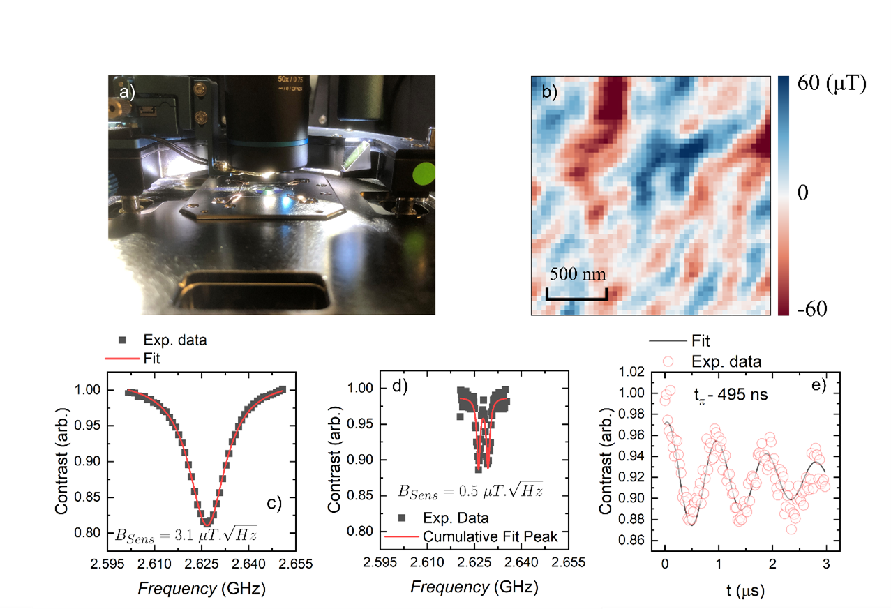
Nitrogen-vacancy (NV) based sensing represents a breakthrough paradigm in characterising advanced quantum material systems. In essence, the NV centre in diamond is a defect within the crystal structure of diamond that possesses the properties of isolated atomic systems and can be utilised as a highly sensitive magnetometer (and thermometer). Combining the NV-sensor into a scanning probe microscope (SPM) creates the ability for spatially resolved quantum sensing of physical phenomena and represents an extremely powerful and versatile measurement tool (Fig a).
Applications can include characterisation of the low-frequency flux noise sources which can result in the dephasing of flux–tuneable qubit devices and quantitative traceable mapping of nanoscale magnetic fields and current density. An example dataset from a pulsed ODMR measurement of a CuMnAs antiferromagnet is shown in Fig b. Here, the exceptional spatial resolution and field sensitivity of the technique is demonstrated. Specific examples of C/W and pulsed ODMR spectra are shown in Fig c and d, and demonstrate the benefits of employing pulsed protocols, minimising microwave and laser broadening, and increasing magnetic field sensitivity.
