Menu
Close
Sign up for NPL updates
Close
Sign up for NPL updates

Receive regular emails from NPL to get a glimpse of our activities and see how our experts are informing and influencing scientific debate

Electromagnetic materials

Advanced characterisation of photovoltaic devices

Photovoltaic metrology and research at NPL

photovoltaics-(1).jpg photovoltaics-(1).jpg

NPL's Photovoltaics team has more than a decade of experience in characterisation and testing for photovoltaics (PV) technologies. Our expertise spans from energy materials characterisation and metrology in the nanoscale, up to PV systems assessment and consultancy. Our multidisciplinary team has led and delivered multiple collaborative R&D projects in the area of PV technologies and has developed a number of novel techniques and bespoke instruments for PV materials, device and module characterisation. We offer a number of established and bespoke characterisation solutions.

Photovoltaic device characterisation capabilities:

  • Standard test conditions (STC) measurements of PV samples up to 10 cm x 10 cm with AAA solar simulator
  • Spectral response and external quantum efficiency (EQE) measurements
  • Photoluminescence imaging with multispectral excitation, for samples up to 20 cm x 20 cm
  • Electroluminescence imaging
  • Photocurrent mapping (photovoltaic cells and modules)
  • Irradiance linearity measurements for solar cells
  • Time resolved photoluminescence (carrier lifetime measurements) (up to 1700 nm emission range), with spatial mapping capability
  • Thermal cycling – damp heat exposure
  • Almost all of our measurement techniques can be performed under inert atmosphere (N2) conditions, and/or controlled oxygen content, using our environmental chambers

photovoltaics-(1).jpgMicroscopy techniques for PV materials and devices:

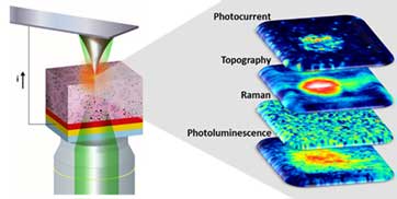
  • Raman spectroscopy
  • Photoluminescence spectroscopy
  • Advanced scanning probe microscopy.
    • Atomic force microscopy (AFM) – topography
    • Scanning kelvin probe microscopy (SKPM) - surface potential, or surface photovoltage
    • Time resolved SKPM – time resolved photovoltage
    • (photo-)conductive atomic force microscopy (pc-AFM, c-AFM) – (photo)current and local current-voltage (in dark or under illumination)
    • Tip-enhanced optical spectroscopy (TEOS) -raman (TERS) and photoluminescence (TEPL).

Custom/bespoke measurements possible (e.g. in-situ studies, temperature control, measurements under controlled atmosphere such inert N2 and very low H2O)

Photovoltaics rating, modelling and system capabilities

  • Uncertainty budgets of measurements
  • Energy rating of photovoltaic modules and devices
  • Albedo estimations for bifacial systems using satellite data sources
  • Albedo on-site monitoring for bifacial systems consultancy

Contact us