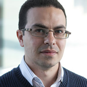
Fernando Castro is Department Head of Science at NPL, leading Advanced Materials and Semiconductors across the lab, with significant experience in working at the interface of academia, industry and government.
Fernando is a renown international expert that plays a leading role in setting the direction of global metrology. He has co-authored NPL’s Technology and Measurement Foresighting (2021), the UK’s Advanced Materials Metrology Strategy (2024), Euramet’s Strategic Research Agenda for Advanced Manufacturing Metrology (2024), contributed to numerous UK strategy documents, and provided expert technical advice to Government and R&D funding agencies in the UK, EU, USA, Sri Lanka, South Korea and Japan.
Fernando holds several distinguished external roles. He is the current Chair of the European Metrology Network on Advanced Manufacturing, established by Euramet for high-level metrology coordination across Europe. Since 2018, he is the UK Head of delegation in the Steering Committee of VAMAS, organisation established by the G7 to accelerate innovation and World trade of advanced materials, where he served as global Chair of VAMAS (2020-2023) overseeing pre-standards research across 15 technical areas involving 300+ organisations in 40+ countries, as chair of Technical Work Area (TWA) 36 Printed Electronics (2014-2020) and as chair of the newly established TWA46 Semiconductors.
Fernando was appointed Visiting Professor at the Faculty of Engineering and Physical Sciences - University of Surrey (since 2018), member of Industrial Advisory Board of the Dyson School of Design Engineering at Imperial College London (since 2023), member of Presidential Board of the World Materials Research Institutes Forum (since 2019), Steering Committee member of the Joint Programme on Photovoltaics of the European Energy Research Alliance (EERA) (2013-2018), Associate Editor of the journal Science and Technology of Advanced Materials (since 2016), and UK expert to the international standards committee IEC TC119 Printed Electronics (2015-current), where he was project leader for the IEC 62899-203-2 ED1 standard.
Fernando has significant experience in leading R&D projects, from small consultancy to large international projects, and has a strong track record of supporting technical innovation in industry leading to demonstrable impact. Among international R&D, he coordinated three large EU projects, and led the International Science and Technology Partnerships (ISPF) project on “Setting the standards for semiconductors” in collaboration with USA, Japan, South Korea and Taiwan.
In the last years, Fernando represented the UK in numerous high-profile meetings, including the UK-South Korea Dialogue on Semiconductors, and the 2nd UK-Taiwan Dialogue on Semiconductors. He led a discussion session for DSIT and KDI with the former Minister of Science and ICT of South Korea, and supported the UK’s National Technology Advisor in meetings with the Deputy Science Minister of Taiwan.
Fernando was the UK lead Expert in Semiconductor in the “UK-South Korea Partnership on Building Capacity Digital Standards and Critical Technologies”, led by UK’s Department for Science, Innovation and Technology (DSIT), the Korea Development Institute (KDI) and Korea’s Ministry of Economy and Finance (MOEF) (2024-2025), which resulted in a high-profile policy report influencing bilateral collaboration.
A prolific author and speaker, Fernando has delivered 80+ invited talks in 20 countries, published 75+ peer-reviewed papers, 3 book chapters, 3 patent families, and several technical reports. He chaired multiple scientific conferences, including the ALTECH series.
He has been the recipient of the NPL’s Rayleigh Award in 2012 and in 2020, which is the highest scientific award at NPL recognising the most outstanding publication of the previous year, and holds several best paper awards from international scientific conferences. In 2023 he was honoured by the Director General of the Council of Scientific & Industrial Research of India (CSIR), for his leadership in advanced materials metrology. He was elected Fellow of the Institute of Physics in 2015 and Fellow of the Institute of Material, Minerals and Mining (IOM3) in 2017.
Emerging semiconductor materials in numerous applications including sensors, photovoltaics, power electronics, wearables and bioelectronics.
Innovation in measurement techniques, in particular for spatially resolved characterisation of functional properties of semiconductor materials and devices at multiple scales (nano, meso, macro)
Advanced scanning probe microscopy (SPM) and optical spectroscopy techniques
Best practice, pre-standards research, standardization methods and protocols for advanced materials and semiconductors
Convergence of critical technologies, foresighting and international coordination
Roadmap on Photovoltaic Absorber Materials for Sustainable Energy Conversion, J.C. Blakesley et al., J Phys Energy 6 (2024) 041501
Minimally Invasive Power Sources for Implantable Electronics, M. Xu et al., Exploration 4 (2023) 20220106
Developing highly reversible Li-CO2 batteries: from on-chip exploration to practical application, M. Wang et al., Energy & Environmental Science 16 (2023) 3960
Overcoming Nanoscale Inhomogeneities in Thin-Film Perovskites via Exceptional Post-annealing Grain Growth for Enhanced Photodetection, T. Du et al., Nano Letters 22 (2022) 979–988
Probing Nanoscale Schottky Barrier Characteristics at WSe2/Graphene Heterostructures via Electrostatic Doping, F. Richheimer et al., Advanced Electronic Materials 8 (2022) 2200196
Emerging bioelectronic strategies for cardiac tissue engineering and cardiac precision medicine, D. Cox-Pridmore et al., Small (2022) 2105281
Multi-scale characterisation of a semi-crystalline polymer reveals hidden ferroelectricity above the Curie transition, J. Hafner, et al., Nature Communications 12 (2021) 152, DOI: 10.1038/s41467-020-20407-6
Integrated contact lens sensor system based on multifunctional ultrathin MoS2 transistors, S. Guo et al., Matter (2021) DOI:10.1016/j.matt.2020.12.002
Nanoscale charge accumulation and its effect on carrier dynamics in tri-cation perovskite structures, D. Toth et al., ACS Applied Materials & Interfaces (2020) 10.1021/acsami.0c10641
Rational Design of Pre-Intercalation Electrodes for Rechargeable Battery, X. Yao et al., ACS Energy Letters 4(3) (2019) 771-778.
Organic photovoltaic cell – a promising indoor light harvester for self-sustainable electronics, H.K.H. Lee et al., Journal of Materials Chemistry A (2018) DOI:10.1039/C7TA10875C
Simultaneous Topographical, Electrical and Optical Microscopy of Optoelectronic Devices at the Nanoscale, N. Kumar et al., Nanoscale 9 (2017) 2723-2731
Spray deposited semiconducting organic single crystals, G.P. Rigas et al., Nature Communications 7 (2016) 13531.
An in-depth analysis on modeling of organic solar cells by using multiple-diode circuits, F.A. Castro et al., Solar Energy 135 (2016) 590-597
Towards reliable charge-mobility benchmark measurements for organic semiconductors, J. C. Blakesley et al., Organic Electronics 15 (2014) 1263-1272.