
.jpg)
See examples below of Intellectual Property (IP) available for licensing and investment.
Sona from the world-leading National Physical Laboratory (NPL), aims to revolutionise breast cancer screening with the world’s first ultrasound-based breast density assessment and monitoring technology, that does not require imaging or trained radiologists.
Early cancer detection is key to saving lives, and sona's unique innovation will ensure women are offered the right forms of screening at the right time.
![]()
 Thermology Health, a spinout from the UK's National Metrology Institute, the National Physical Laboratory (NPL), is revolutionising diagnostic healthcare through thermal imaging.
We are focused on the development of robust and reliable thermal imaging measurement in healthcare applications. Our technology delivers medically relevant levels of temperature measurement (±0.2°C), unlocking the huge clinical diagnostic and prognostic potential of thermal imaging in health, for the first time. It uses technology to target diabetes related foot amputations.
NPL has developed a new class of high-accuracy coordinate measurement system aimed at the next generation of automated manufacturing applications, such as metrology assisted machining and assembly. The system operates conceptually like global navigation using GPS; with sensors surrounding the working volume, simultaneously detecting multiple points of interest.
.png?lang=en-US&uh=19316f141f73d2d006a4b68f199667b0d6a1feee90ea382b3b8c44991819e25a)
The K3M system has several key advantages over the current state-of-the-art:
Manufacturers that require high-accuracy, flexible metrology systems, that can be easily embedded in their processes.
Born from cutting-edge research from the National Physical Laboratory, HIDRA Vision is spearheading a revolution in inspection technology for the future of the semiconductor industry. As semiconductor manufacture approaches the limits of silicon technology and continues to drive the adoption of new materials, packaging and optical integration, there is an inescapable need for advanced wafer inspection and yield management approaches.
Conventional semiconductor wafer inspection relies on point sampling, which takes time and cannot test the entire wafer. This results in only around 1% of a wafer being tested, leaving blind spots where defects can escape undetected. This leads to poor yield management and wafer rejection, creating losses and mistrust across the supply chain. As these wafers increase in size and complexity, even a single defect can lead to staggering losses, making this outdated approach no longer acceptable.
HIDRA Vision’s groundbreaking technology solves this issue by providing true 100% full-wafer inspection without sacrificing throughput or accuracy. Our solution provides a real-time, data-driven process control and equips manufacturers with the critical insights to make informed business decisions based on die performance and continuously improve their manufacturing processes.
Compound semiconductors currently represent a $43B market with 11% CAGR over the next decade. Compound semiconductors offer superior performance than silicon in particular for applications with high voltage, high speed and photonic endpoints, such as facial recognition, datacom, LiDAR, power, RF and lighting.
HIDRA vision is seeking external investment to create a spinout company that will seek to access this multi-billion dollar market.
Optical interferometry is a technique using the interference of two electromagnetic waves that can make accurate measurements of displacements. It is a fundamental technology in the traceability chain for length metrology. Almost all length measurements that are traceable will have an optical interferometer measurement somewhere in their traceability chain. Various high level strategic studies of needs for nanoscience have highlighted the need for precision measurements, some of which are interferometry based, to support nanotechnology. Accurate dimensional nanometrology is crucial for determining an object’s location as well as its dimensions and often larger macroscale objects or displacements need to be determined with nanometre accuracy.
NPL has expertise and intellectual property in the areas of opto-mechanical interferometer design for a variety of applications using bespoke interferometer designs, signal collection and processing using hardware and software, application of routines to minimise the effects of mechanical instability, non-linearity and atmospheric fluctuations as well as calculation of measurement uncertainty. NPL Optical Interferometer technologies can achieve positional accuracy at the sub-nanometre level, with a high bandwidth and significantly lower non-linearity than commercial systems.
The ever-increasing take up of nanotechnology from the research laboratory into industrial applications will be important for realising the new technologies in critical sectors identified by the UK Government such as semiconductor manufacturing and quantum technologies. In these sectors, accurately and repeatably knowing the position of an object and its dimensions to nanometre and sub-nanometre levels is crucial to enabling next generation fabrication, processing, quality assurance and control.
Instrument manufacturers with requirements for ultra-high precision positioning.

 What is the technology?
This technology delivers accurate power readings in low temperature environments.
Getting an accurate reading for microwave power in cryogenic environments is becoming increasingly important in fields such as quantum computing, quantum sensing and materials research. However, getting an accurate reading of the microwave power delivered to devices at ultralow temperatures can be very challenging and time-consuming. The quantum microwave power meter relates to power sensors for measuring absolute power of microwave signals in cryostats. The invention relates to measurements of the absolute power of propagating monochromatic microwaves in the range of 1 – 20 GHz at temperatures of less than 100 mK with help of a quantum mechanical sensor. It can be applied to calibration coaxial cables and cryogenic devices.
To our knowledge, there are no other methods of measuring microwave powers inside at low temperatures inside the dilution refrigerators. The proposed power meter allows you to detect the absolute power using basic principles of quantum mechanics. The quantum microwave power meter means that swift broadband, non-invasive, in-situ measurements of microwave power can be made along any transmission line in cryogenic environments. Its small footprint allows for seamless integration in series with existing microwave circuitry, and when not in use the power meter can be switched off so it does not to impact any of your measurements. This can be done without having to warm up the cryostat or make any changes to the setup.
The rise of quantum technologies will require more strict control and manipulation of quantum states. Much of this manipulation is performed using microwaves at cryogenic temperatures. There is an immediate need to develop methods to quantify and calibrate the performance of microwave components and devices at cryogenic temperatures. Today it is not feasible for microwave component manufacturers to calibrate and specify their devices at cryogenic temperatures. Target markets are:
quantum computing
This technology enables the development of sensitive sensors.
NPL has invented a novel way of conducting interferometry, a measurement method using the phenomenon of interference of waves. It is based on a continuous matter wave beam splitter which allows multiple laser beams to be arranged to form waveguides.
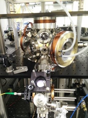 Atomic interferometers are similar to optical interferometers, except they use matter waves instead of optical ones. All interferometers rely on the formation of interference fringes due to interference between partial waves, which propagate along different pathways. The spatial position of the interference fringes depends strongly on relative phases of the interfering partial waves, which makes interferometers very sensitive to different perturbations. Atoms, compared to massless photons, have relatively large mass, so atom interferometers are very sensitive to the gravity, inertial and electromagnetic forces. For that reason, atom interferometers are used now for different inertial quantum sensors, like gravimeters, accelerometers and gyroscopes. Most existing atom interferometers are using laser-cooled atomic clouds, which are free falling in gravity inside vacuum chambers.
At NPL we are working on developing integrated optically guided atomic interferometers, based on all-optical atom chips. Such interferometers should provide compactness of quantum inertial sensors without compromising their sensitivity and accuracy.
It is inherently suitable for exploitation in a range of products, such as sensors, at an affordable price. For example, transportable precise gravimeters used in civil engineering, geological surveys, earth studies and control of sea levels and climate changes. It can also be used in the application of inertial sensors for inertial navigation of vehicles, especially in absence of other means for navigation.
It is a novel system that employs telecoms laser light in an all-fibre based optical system. Counter-propagating laser beams are coupled into a microresonator via an integrated tapered fibre. This straightforward configuration allows the manipulation of light in a reproducible and controlled manner through the relative adjustment of the relative power of each beam. This technology enables a number of different applications from optical gyroscopes to chip based spectroscopy and advanced optical sensors.
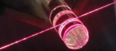
NPL has developed and patented unique microresonator technology which can be used for sensors, accelerometers and spectroscopes.
This technology has the ability to take magnetometers to a new level of sensitivity.
NPL has developed a novel mode of operation of the radio-frequency atomic magnetometer, the so-called spin maser. The mode relies on the spontaneous fluctuations of the atomic spin being optically monitored and the signal from the optical detection fed back to the atomic sample.
 The magnetometer emits a radio wave to the object under test. This interacts with the material and generates an eddy current and secondary magnetic field which is picked up by the magnetometer as quantum level changes that are measured optically. This allows the shape of the material to be derived.
Standard non-destructive testing and detection of ferromagnetic objects relies on magnetic inductive tomography using atomic magnetometers, but suffers from the radio frequency resonance shifts induced by the tested objects. This means measurements are often less accurate than required. NPL’s spin maser technology solves that problem and enables more accurate measurements with a significant reduction of the image acquisition time.
The higher accuracy, fast acquisition time and non-destructive nature of the testing are all key benefits over current methods and equipment.
It has the potential to be used in a wide range of industrial applications including detection of corrosion under insulation, a critical problem for industrial plants, or in medical devices and security applications.
NPL has developed a novel solution to the problem of detecting small differences in images over time. Digital image correlation can show degradation in the assets or patients surveyed by capturing an initial image and this forms the baseline. Then an image can be captured at some point in the future, to show the current state. Comparing one against the other, pixel by pixel, enables changes to be identified with unprecedented accuracy.
Digital image correlation is a unique method of comparison based on advanced algorithms that has the potential to benefit a range of industries requiring regular inspection of changes to status, from railway tunnel inspection and nuclear containment facilities to medical diagnostics. It is a breakthrough in the detection of subtle changes.

This technology enables measurement of electrical characteristics of thin films.
We have developed technology for graphene measurements which means we are able to perform a sheet resistance or equivalently electrical conductivity characterisation of thin graphene and other films with lateral spatial resolution in the range from centimetres down to micrometres allowing us to characterise it.
This unique method is not only applicable to graphene but also other thin conducting films. We plan to offer technical solutions for future roll-to-roll production facility in-line metrology as demand increases. This will enhance productivity and quality control of industrial processes.
As well as sheet resistance our patent also covers measurement of electrical mobility and carrier concentration in thin conducting films, using an extension of the basic technology with the addition of a magnetic field. This non-contact approach is a unique capability within the UK.
This technology will be of interest to anyone working with thin films such as in graphene production.

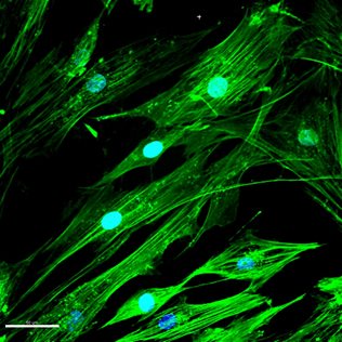
SANET is a unique synthetic peptide that NPL has developed that has the potential to be used as an extra cellular membrane (ECM) to provide structural function in cells and aid in tissue growth and repair.
Cells incubated with SANET could be used to create synthetic replacements for current animal derived ECMs, which is important for applications like in vitro drug studies.
NPL has filed a patent against our specific sequence.
This technology would be of interest to medical companies and researchers currently using extra cellular membranes and wish to have the benefits of synthetic ECMs.
UK public sector organisations are leading and enabling a new generation of radical innovations. The expertise found within science laboratories is driving ground-breaking research and development and delivering these game-changing ideas into the hands of the customers. NPL hosted three webinars demonstrating the parallels between real-life applications and the global issues facing society. They highlighted how collaboration between the public and private sector can accelerate the development of new technologies to keep us all healthy, reduce pollution, explore space and more.
Since its establishment in 1900, NPL has been delivering innovations to improve prosperity and quality of life for those living in the UK. In the late 1960’s NPL invented packet switching, a key ingredient of the internet, and this was then further developed into general computing and ultimately quantum computing. The Kibble balance, formerly the watt balance and renamed after Bryan Kibble who worked at NPL, was developed in the 1970s. It compares electrical and mechanical forces, which allows the kilogram to be realised in terms of quantum electrical units.
More recently, NPL has been involved in metrology and characterisation of graphene to facilitate the commercialisation of graphene. The world’s first room temperature maser, which produces monochromatic electromagnetic radiation in the microwave range, was invented at NPL and is used in atomic clocks. We have developed a way of using existing optical fibres in our communications infrastructure to detect seismic activity – an innovative use of existing technology. NPL has also worked in collaboration with companies and universities to support innovations as diverse as graphene-based sensors to radiation treatment for medical equipment.
Our research and measurement solutions support innovation and product development. We work with companies to deliver business advantage and commercial success.
Contact our Customer Services team on +44 20 8943 7070