
 The low-temperature nanoprobe is a state-of-the-art system suitable for surface topography imaging with atomic resolution, density of states mapping and electrical characterisation of thin films, nanostructures and devices. It ranges from microns down to the atomic scale. Electrical characterisation is achieved via multiprobe transport measurements supported by the extremely accurate probe positioning. The instrument can probe a wide range of materials, from conventional metals and semiconductors, to novel nano and quantum materials. Structural and electrical information, such as conductance and impedance, is important for the semiconductor industry. The instrument can also be used for fundamental studies and applications, such as material growth control and validation or surface homogeneity. Studies of surface reactions at the atomic level are particularly useful for catalysts and gas sensing applications, as well as single-atom impurities and defects.
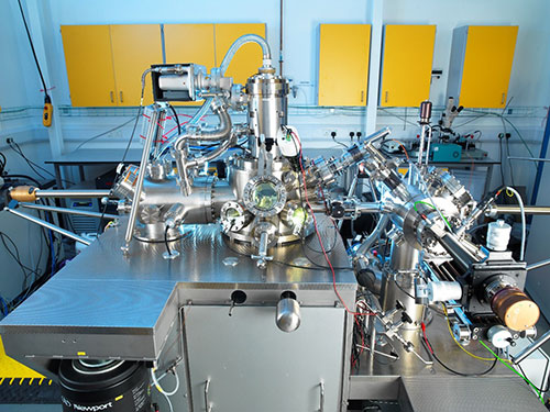
The low-temperature nanoprobe UHV system (Scienta Omicron Technology GmbH) is equipped with 4 independently controlled probes, suited for scanning tunnelling microscopy, QPlus atomic force microscopy and electrical transport measurements (with two of the probes capable of microwave measurements). The operating temperature of the system ranges from ~4K to room temperature. A high-resolution scanning electron microscope (SEM) column is used for tip navigation and in-situ imaging (5-20 keV). The system features an optical fibre for sample illumination, 25mT out-of-plane magnetic field and additional contacts on the sample platform for back-gating. The preparation chamber capabilities include resistive/e-beam heating/annealing, Ar sputtering, e-beam deposition and tip preparation.