Direct imaging of subwavelength mid-infrared light in metal-dielectric nanoantenna arrays
The aim of the project was to design, fabricate and demonstrate proof-of-concept nanoantenna arrays, which resonantly couple to light of a desired wavelength in the mid-infrared (IR).
Within the University of Glasgow’s quantum enhanced imaging hub (QuantlC) , NPL’s QMS group have collaborated with Imperial College London to directly image nanoscale light in custom-built metal-dielectric nanoantenna arrays. This project combines Imperial’s design and fabrication expertise with the scanning near-field optical microscopy (SNOM) measurement capabilities of NPL.
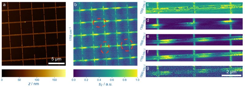
In discussions between NPL and Imperial, we settled on a gold-glass photonic crystal design, targeting a wavelength 5.75 μm (or ~1740 cm1). The array layout was formed of waveguides with periodic, perpendicular nanoantennas, designed to couple in the far-field light (see (a)). Finite difference time domain (FDTD) modelling was used to design an array of nanoantennas, then several samples with slight variations were produced in the clean room at Imperial.
SNOM measurements allowed direct imaging of the subwavelength light with nanometre resolution. We validated the initial modelling, demonstrating that close to the target wavelength, the arrays behaved as designed, with guided modes propagating along the waveguides (see (b)). We further studied the dependence of the behaviour on wavelength (see (c-g)). Similar behaviour was observed at 1755 and 1600 cm-1, evidence that the far-field coupling has a low quality factor. At wavelengths further from the one targeted, we observed deviation from the designed behaviour, indicating a reduced coupling efficiency.
We also noticed interesting deviations from the periodic behaviour, localised at fabrication defects in the arrays (circled in (b)). This prompted us to image areas at the array edges, which may allow us to distinguish optical contributions from the crystal unit cell, and from its periodicity. The local effects of these defects could be studied further by deliberately including defects in pristine arrays.
After this successful proof-of-concept, we intend to work towards repeating this process using dual mode arrays. These could enable technologies such as spontaneous photon down conversion (SPDC) in the mid-IR, allowing generation of single photons and entangled photon pairs, which could be exploited for future quantum imaging applications.

Near-field imaging of nanoscale light in photonic crystals. (a) AFM topography map showing horizontal waveguides and vertical antennae. (b) Corresponding 2nd harmonic near-field light amplitude (s2) at 1755 cm1, showing anomalous behaviour at defects (circled). (cg) Wavelength resolved SNOM images from a smaller area of the crystal, showing breakdown of the periodicity at 1000 cm1. Scale bars shared by a and b, and c-g.