
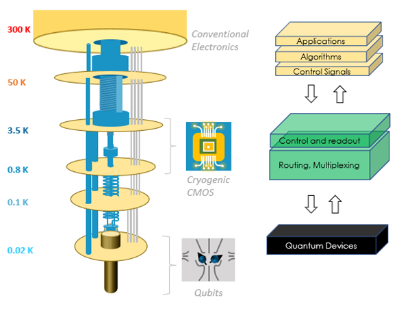
The advanced nature of established silicon fabrication capabilities and supply chains offers a unique opportunity to develop novel quantum technologies. Silicon is a promising material for quantum components, and silicon-based transistors can be used as quantum devices or as custom cryogenic logic modules for dedicated control circuitry in quantum computers.
When silicon devices are used as quantum devices, such as spin qubits, they require different control and optimization techniques than classical bits. This is because quantum devices are sensitive to environmental noise and require operation in a deep cryogenic environment. Specialised device readout techniques, such as charge sensors and reflectometry, are also needed to measure the state of quantum devices.
Characterising the building blocks of cryogenic logic and control circuits is another critical area. Although this is closer to traditional methods, cryogenic conditions, power dissipation limits, and demanding performance requirements make this a non-trivial task.
The National Physical Laboratory (NPL) is working on projects that use commercial silicon fabrication platforms to develop quantum devices and cryogenic control electronics. These projects are part of the "stack" of technologies that are needed for scalable quantum information processing.
To assist the integration of these technologies NPL are developing tests customised to cryogenic silicon challenges.
NPL’s scientists have extensive experience in quantum electrical metrology. They operate sophisticated cryogenic facilities with extensive low noise electrical measurement and radio frequency (RF) techniques. As the UK’s National Measurement Laboratory they also have access to state-of-the-art calibration systems. They regularly collaborate with laboratories around the world including NTT, NIST, PTB, KRISS, UNSW.
The National Physical Laboratory (NPL) is a partner in the ISCF project Altnaharra, led by Quantum Motion. This project aims to create a custom-designed chip for integrated qubit control and readout, fabricated in a CMOS (complementary metal-oxide-semiconductor) foundry. NPL is helping to define the device parameters and test fabricated circuit modules. In particular, we are conducting detailed electrical characterization to optimise operation at lower temperatures.
.jpg")
Photograph of a silicon CMOS Chip
Our team has a diverse range of expertise and access to advanced characterisation tools:
NPL is an active participant in the field of semiconductor-based quantum technology, for example in the validation of quantum electrical standards or fundamental studies of semiconductor device physics. For instance, our teams have performed a controlled collision of single electrons in a semiconductor chip.
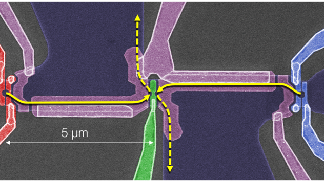
Collision of single electrons published in Nature Nanotechnology
NPL is keen to work with industrial partners. If you are interested to see how you could collaborate with NPL to support the development of technologies please get in contact.