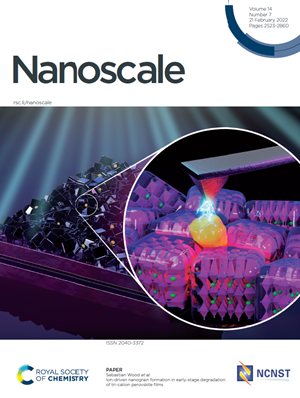
In emerging electronic technologies, the nanoscale structure is increasingly understood to play a critical role in the performance of devices. The development of nanoelectronics has been driven by ongoing miniaturisation of components, below the 10 nm scale, and the emergence of new electronic materials exhibiting nanoscale features.
NPL has developed world-leading scanning probe microscopy (SPM) nanometrology facilities for the measurement of electronic materials, with a focus on linking local structural characteristics to functional performance. These facilities are currently being used to support UK industry and academic partners throughout various development stages of disruptive electronic products, including IR sensors, solar cells, power electronics, and LED technologies.
A recent study, published in Nanoscale, focused on understanding the origins of early-stage degradation behaviour in organic-inorganic perovskite semiconductor thin films which are used for high efficiency next-generation solar cells. Despite attracting significant interest, these materials exhibit operational instabilities, which need to be addressed in order to match lifetimes of current commercial solar modules. Using the unique capabilities of NPL’s nanometrology platform, the formation of nanoscale surface grains was identified as a sign of early‑stage degradation. The origin of this effect was further linked to the local electronic and ionic charge environment when exposed to simulated solar cell operational conditions. By identifying the nanoscale origin of the degradation mechanism, targeted passivation strategies can be designed to contain this effect. Increased control over the operational instabilities of this next-generation photovoltaic technology will help to accelerate its commercial uptake for conventional photovoltaics and alternative markets, which include sensors, building and vehicle integrated solar and internet of things. 
Earlier this year another study was published in Nano Letters, where scientists led by Queen Mary University of London identified a treatment effective in eliminating performance limiting defect clusters in organic-inorganic perovskite semiconductor thin films. With the help of advanced nanoscale-resolved (photo-)current measurements carried out by NPL scientists, the presence of such defect clusters in untreated films was resolved. In addition, the positive impact of the new post-deposition treatment was quantified as leading to a 20- to 40-fold increase towards low-light detection capability, enabling the development of photodetectors with higher light sensitivity. This is an important study to improve perovskite deposition processes, in which the team were able to have an important role in quantifying the overall impact in applying that treatment method.
These recent studies demonstrate how NPL’s nanometrology capability underpins scientific innovation and industrial uptake of next-generation optoelectronic materials. NPL maintains and develops cutting-edge measurement techniques and facilities that enable industry and society to exploit and innovate swiftly and safely.
Find out more about our work in emerging electronic materials here: www.npl.co.uk/electronic-magnetic-materials
image courtesy of Nanoscale journal.
04 Mar 2022