
Materials characterisation and imaging is the study of how materials are structured, what they are made of, and how they behave. This includes understanding how atoms are arranged and how this affects a material’s properties.
At very small scales, scientists need techniques that go beyond optical microscopes, which cannot resolve very tiny features. Instead, they use advanced methods to study materials at the nanoscale and even down to individual atoms.
This information is essential for developing new technologies, for example improving electronic devices, designing better materials, and creating advanced medical applications.

Traditional light microscopes are constrained by the optical diffraction limit, which means they cannot resolve features smaller than about 200 nm. Many modern materials, such as those used in quantum technologies and electronics, have important features far smaller than this. In 2025, ultra-narrow semiconductor metal tracks manufactured as close as 24 nm enable high performance.
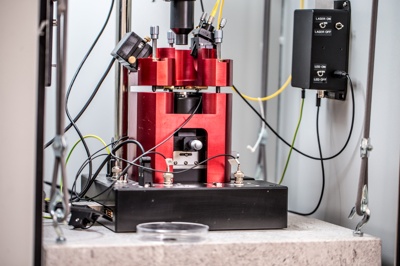
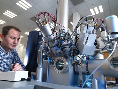
NPL uses specialised nanoprobe facilities and a variety of techniques to image and measure materials from the nanoscale down to the atomic scale. We combine advanced microscopy with measurement science to ensure results are accurate, repeatable and traceable, supporting both research and industry.
AFMs do not use light. Instead, a tiny sharp probe moves across a surface and “feels” it using very small forces between atoms. A laser system detects how the probe moves, allowing NPL to map surface shapes with sub-nanometre precision. Variations of AFM can also measure properties such as heat flow at the nanoscale.
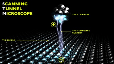
STMs allow scientists to image materials atom by atom. A conducting tip placed extremely close to a surface causes a small electrical current to flow due to quantum tunnelling. By measuring this current, NPL can map atomic positions and electronic properties of materials.
Seeing a material’s surface is not enough to understand how it works. NPL combines imaging with spectroscopy techniques to identify what a material is made of. Methods such as AFM infrared spectroscopy and Secondary Ion Mass Spectrometry allow NPL to map chemical composition and impurities in three dimensions.
For technologies such as quantum sensors and spintronics, magnetic behaviour at very small scales is crucial. NPL uses magnetic force microscopy to map tiny magnetic domains, helping researchers understand and improve magnetic materials used in information storage, biomedical research and quantum materials.
NPL controls probe motion using piezoelectric materials, which change shape when a voltage is applied. By adjusting the voltage by tiny amounts, probes can be moved by fractions of a nanometre. This smooth, continuous motion is essential for atomic scale imaging.
Piezoelectric materials can behave slightly differently depending on their history, an effect called hysteresis. NPL overcomes this by using closed loop measurement systems that continuously monitor the probe’s real position and correct it in real time. This ensures stable, accurate measurements over long experiments.
Accurate characterisation and imaging allow scientists and engineers to understand materials at their most fundamental level. By providing trusted measurement science that can combine information collected by several methods, NPL helps turn new materials and devices - from quantum technologies to advanced electronics - into reliable, real-world applications.
Our research and measurement solutions support innovation and product development. We work with companies to deliver business advantage and commercial success.
Contact our Customer Services team on +44 20 8943 7070