Validation techniques
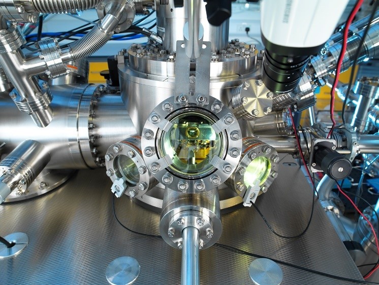 Low-temperature 4-probe scanning tunnelling microscope
We develop:
- Robust measurement for characterisation of materials
- Non-destructive testing and evaluation methods for quality assurance
- Physical measurement methods utilising material and sensor innovation to accelerate process development and improve quality control
Reliable methods to determine the quality and physical properties of quantum materials are vital to their widespread inclusion in practical devices with novel functions. We use a wide suite of tools to characterise these materials in terms of their properties.
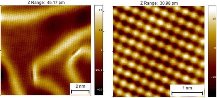 Atomically resolved surfaces by STM and qPlus AFM
Structural properties – With our Atomic Force Microscopy (AFM), Scanning Tunnelling Microscopy (STM) and confocal Raman spectroscopy facilities, we can measure a variety of the structural properties of quantum materials, such as material thickness, coverage, defect state and strain.
Electric and electronic properties – We can probe properties such as surface potential, carrier density distribution, band structure, sheet resistance and electrical transport with techniques including Kelvin Probe Force Microscopy (KPFM), van der Pauw and Hall measurements, FET measurements (including Dirac point and conductivity vs. gate voltage), microwave resonator techniques and our conventional four probe and state of the art ultra high vacuum (UHV) four-probe STM system.
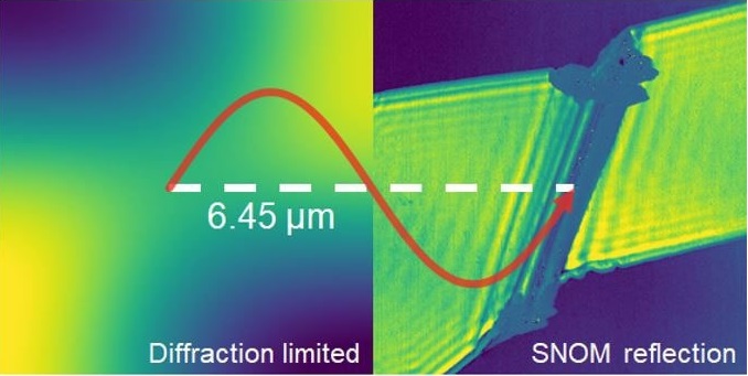 Diffraction-beating imaging using SNOM
Optical properties – Our suite of optical techniques, including Raman and photoluminescence spectroscopy, as well as Scanning Near Field Optical Microscopy (SNOM), can measure the optical properties of quantum materials from the visible to the infrared.
Thermal properties – We measure the nanoscale thermal conductivities of a range of samples using Scanning Thermal Microscopy (SThM), in both ambient conditions and vacuum, and Nanoscale Thermal Analysis (nanoTA).
Chemical properties – With Raman and photoluminescence, we can distinguish and characterise many different quantum materials, using a mixture of spectroscopic analysis and spatial mapping of sample composition. Additionally, we can identify and pinpoint various chemical species, such as functionalised groups on graphene, with nanoscale spatial resolution using AFM-infrared spectroscopy (AFM-IR).
Some highlights of our research include:
- Resolving nanoscale infrared domains at hBN-Graphene Interfaces
- Thermal Conductivity of Atomically Thin Materials by Scanning Thermal
Microscopy - Contactless probing of graphene charge density variation in a controlled humidity environment
- Demonstrating that band alignments and luminescent properties of heterostructures can be controlled by the underlying substrate
- The effect of charged impurities on the electronic transport of hexagonal boron nitride-encapsulated graphene
- Detecting ultralow concentration NO2 in complex environment using epitaxial graphene sensors
- Graphene as an ideal material for a quantum resistance standard
Contact us
Our research and measurement solutions support innovation and product development. We work with companies to deliver business advantage and commercial success.
Contact our Customer Services team on +44 20 8943 7070