6GOnWafer
Advancing traceable measurements for future 6G technologies

The European Chips Act aims to strengthen supply chain resilience and increase Europe's share of the global semiconductor market from 10% to 20% by 2030.
Emerging technologies such as 6G communications, automotive radar and satellite-based climate monitoring increasingly rely on millimetre-wave and sub-terahertz (30 GHz to 300 GHz) frequencies. However, there is currently no established SI-traceable approach for many of the measurements needed to characterise devices operating at these frequencies.
One of the key measurements is the S-parameter, which describes how high-frequency signals travel through electronic components and circuits. These measurements are vital for technologies such as on-chip antennas, differential circuits and complex multiport semiconductor devices. At high frequencies, internally generated noise can limit the performance of transistors, amplifiers and receivers.
Building on the earlier PlanarCal, TEMMT and OnMicro projects, 6GOnWafer will develop the first traceable and validated techniques for measuring on-wafer 6G antennas up to 330 GHz. The project will also establish traceability for multiport and differential circuits, develop on-wafer noise measurements up to at least 110 GHz, and improve traceable measurements of substrate materials at temperatures up to 150 °C and frequencies of at least 220 GHz.
The project will provide the measurement infrastructure needed to support future semiconductor technologies and accelerate the development of emerging applications, including 6G communications.
The knowledge generated through the project will be used to develop good practice guidance for industry and researchers, helping Europe strengthen its semiconductor capabilities and meet the ambitions of the European Chips Act.
This project is running from June 2026 to May 2029.
Project aims
The overall aim of 6GOnWafer is to develop traceable and validated measurement techniques for advanced semiconductor devices operating at millimetre-wave and sub-terahertz frequencies.
The project will help establish the measurement infrastructure needed to support future technologies, including 6G communications, highly automated vehicles, space applications and next-generation electronics. It will also strengthen Europe's capability in semiconductor measurement science and support the development of a coordinated European metrology infrastructure.
The project has five objectives:
1. Improve traceable measurements for complex semiconductor circuits
Develop traceability and verification techniques for multiport and differential on-wafer S-parameter measurements at frequencies up to 220 GHz. This includes investigating calibration methods that reduce crosstalk effects and producing guidance to support accurate measurements of complex on-wafer circuits.
2. Develop traceable measurements for on-chip antennas
Establish traceability and verification techniques for the measurement of connectorless 6G antennas, including on-chip antennas, at frequencies up to 330 GHz. The work will assess the influence of measurement probes and evaluate both established and emerging field-mapping techniques.
3. Establish traceable on-wafer noise measurements
Develop traceable and validated methods for measuring the noise figure of planar semiconductor devices, such as transistors, at frequencies up to at least 110 GHz.
4. Improve material characterisation and defect detection
Develop accurate and traceable techniques for characterising microwave substrates, including semiconductor wafers, at temperatures up to 150 °C. The project will also investigate methods for detecting defects in semiconductor wafers at frequencies up to at least 220 GHz.
5. Create impact across industry and research
Support the adoption of the project's measurement methods by industry, national metrology institutes, calibration laboratories, standards organisations and the wider semiconductor and communications sectors.
Project structure
The project is organised into five work packages covering measurement traceability, antenna characterisation, noise measurements, semiconductor materials and industry impact.
WP1: Traceable on-wafer S-parameter measurements for complex circuits
Lead partner: VSL
Multiport and differential circuits are increasingly used in applications such as 6G communications, automotive radar and optical and quantum technologies. However, established traceable measurement methods are currently lacking for multiport and differential on-wafer devices, particularly at millimetre-wave frequencies
This work package will develop traceable and validated measurement techniques for multiport and differential on-wafer S-parameter measurements at frequencies up to 220 GHz.
Key activities
- Develop calibration and verification substrates for complex circuit measurements.
- Investigate calibration methods that reduce crosstalk between measurement probes.
- Develop traceable measurement techniques for multiport devices.
- Develop traceable measurement techniques for differential devices.
- Produce guidance to support accurate and repeatable measurements.
Expected outcome
Improved confidence in measurements of advanced semiconductor circuits operating at millimetre-wave frequencies.
WP2: Traceable measurements for on-chip antennas
Lead partner: LNE
On-chip antennas are expected to play an important role in future 6G systems. This work package will develop traceability and verification techniques for both antenna measurements and field-mapping methods at frequencies up to 330 GHz.
Key activities
- Develop traceable S-parameter measurements for on-chip antennas.
- Design and test calibration standards and verification devices.
- Assess measurement uncertainties and probe effects.
- Develop and evaluate field-mapping techniques for antenna characterisation.
- Compare different measurement approaches through an interlaboratory study.
Expected outcome
Improved measurement traceability and reproducibility for on-chip antenna technologies.
WP3: Traceable on-wafer noise measurements
Lead partner: NPL
As semiconductor devices operate at increasingly high frequencies, understanding and measuring noise becomes more important. This work package will establish traceable methods for measuring noise figure in planar semiconductor devices at frequencies up to at least 110 GHz.
Key activities
- Investigate the theoretical principles and assumptions underpinning on-wafer noise figure measurements
- Develop SI-traceable on-wafer noise figure measurement systems operating up to at least 110 GHz
- Quantify and document measurement uncertainty.
- Measure noise performance in representative devices.
- Compare results across participating laboratories.
Expected outcome
The first traceable interlaboratory comparison of on-wafer noise figure measurements.
WP4: Traceable microwave substrate measurements over temperatures and defect inspection in semiconductor wafers
Lead partner: TÜBİTAK
This work package focuses on both semiconductor material characterisation and defect detection.
- Develop traceable methods for characterising semiconductor substrates and microwave materials at temperatures up to 150 °C
- Improve understanding of material properties at frequencies up to at least 220 GHz
- Investigate non-destructive techniques for identifying defects in semiconductor wafers
- Evaluate and compare different inspection methods and their associated uncertainties.
Expected outcome
Improved measurement capability for semiconductor manufacturing, material characterisation and quality assurance.
Consortium

6GOnWafer brings together national metrology institutes, research organisations, universities and industrial partners from across Europe and beyond. The consortium combines expertise in semiconductor measurement science, microwave metrology, antenna characterisation and advanced electronics.
National metrology institutes
- National Physical Laboratory (NPL), United Kingdom
- Czech Metrology Institute (CMI), Czechia
- Central Office of Measures (GUM), Poland
- Laboratoire national de métrologie et d'essais (LNE), France
- Federal Institute of Metrology (METAS), Switzerland
- TÜBİTAK National Metrology Institute (UME), Türkiye
- VSL National Metrology Institute, Netherlands
- National Metrology Centre (NMC), Singapore
- Korea Research Institute of Standards and Science (KRISS), Republic of Korea
Research and academic partners
- Chalmers University of Technology, Sweden
- Centre national de la recherche scientifique (CNRS), France
- Czech Technical University (CTU), Czechia
- Ferdinand-Braun-Institut (FBH), Germany
- University of Glasgow (UofG), United Kingdom
- Université de Lille (ULILLE), France
- Brandenburg University of Technology (BTU), Germany
Industrial partners
- Anritsu, Austria
- FormFactor, Germany
- Keysight Technologies, Belgium
- Anteverta (Maury Microwave Europe), Netherlands
- Rohde & Schwarz, Germany
- STMicroelectronics Crolles, France
- MPI Corporation, Taiwan
Outputs
Project outputs will be published throughout the lifetime of 6GOnWafer. These will include technical publications, conference presentations, workshop materials and guidance developed through the project.
Publications
Research papers, technical reports and other project publications will be listed here as they become available.
Workshops and events
The project will organise and contribute to workshops, conferences and other knowledge-sharing activities. Details of upcoming events and presentation materials will be added here.
Guidance and best practice
The project will develop guidance to support accurate, traceable and reproducible measurements for semiconductor devices and emerging 6G technologies. Relevant documents will be made available as they are published.
News and events
Follow this page for the latest updates from the 6GOnWafer project, including project milestones, publications, events and technical achievements.
Project kick-off meeting held at NPL
The 6GOnWafer project officially launched with a kick-off meeting at NPL in Teddington on 17 and 18 June 2026. Hosted by project coordinator Xiaobang Shang, the meeting brought together 35 participants from across the consortium, both in person and online.
Discussions focused on the project's objectives, technical work packages and plans for the first phase of research. The meeting provided an opportunity for partners to align priorities and begin collaborative work on developing traceable measurement techniques for future semiconductor and 6G technologies.
Follow 6GOnWafer on LinkedIn
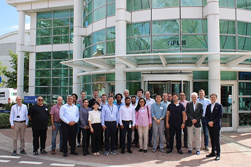
Photo: Participants at the 6GOnWafer kick-off meeting hosted by NPL.
Contact information
For further information on the project, please contact Xiaobang Shang, project coordinator.
Funded by the European Union. Views and opinions expressed are however those of the author(s) only and do not necessarily reflect those of the European Union or EURAMET. Neither the European Union nor the granting authority can be held responsible for them. The project has received funding from the European Partnership on Metrology, co-financed from the European Union’s Horizon Europe Research and Innovation Programme and by the Participating States.

Contact us
Our research and measurement solutions support innovation and product development. We work with companies to deliver business advantage and commercial success.
Contact our Customer Services team on +44 20 8943 7070